PC/104p-BiSerial-III
PCI-104, PC/104p, PC104+ Compatible
RS485, LVDS, ADC and DAC State-Machine IO
Full and Half Duplex Serial / Parallel Data Interface with DMA
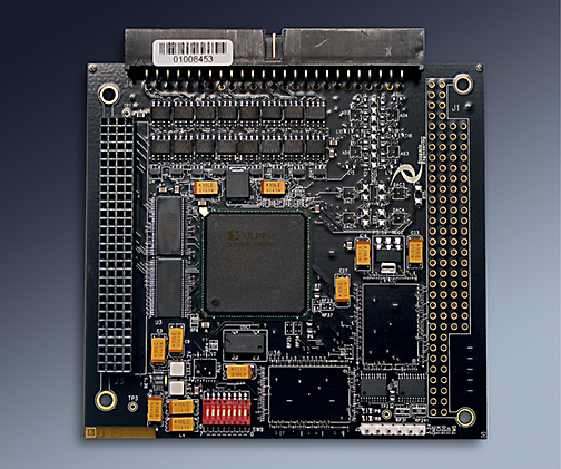
Front View
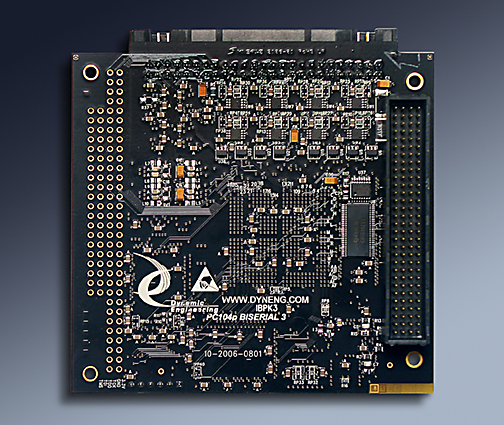
Rear View


| Standard PCI-104 or PC/104p |
|
| |
|
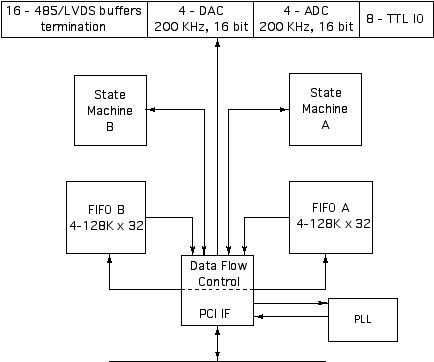
| 40 MHz RS485 signaling supported. LVDS transceivers rated at 200 MHz. Xilinx may limit the top rate, 200 KHz ADC, 200 KHz DAC, TTL is Xilinx driven. |
|
| |
|
| PLL [Cypress 22393], PCI, OSC, External clock sources are available for use |
|
| |
|
| Standard 33 MHz. operation. Standard 32 bit operation. Independent DMA support for each TX and RX channel available |
|
| Registers are read-writeable. Transmit and Receive functions separated. | |
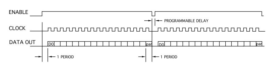
| Transmit and Receive state-machines, FIFO Programmable almost empty [transmit] and programmable almost full [receive] have programmable interrupts. Status can be polled for non-interrupt driven operation as well. |
|
| |
|
| 16 RS-485 / RS-422 compatible IO are provided. Any combination of transmit or receive channels can be created. Programmable termination. LVDS IO are available on all channels. Up to 4 DAC channels and/or 4 ADC channels can be added. Each channel can operate at 200 KHz and has a 16 bit resolution. 8 TTL IO are provided. |
|
| |
|
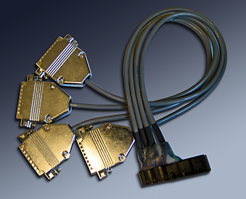
| The IO is available via the 50 pin right angle header. The differential IO is properly routed with controlled spacing and matched lengths on each of the pairs. Custom cables are available. |
|
| |
|
| Custom programmed interfaces are available, standard options are shown below. |
|
| +5, 3.3, 2.5, 1.2. 3.3, 2.5 and 1.2 converted with on-board regulators. |
|
| Separate external FIFOs are options. 4K, 8K, 16K, 32K, 64K, and 128K x 32 are available. Internal FIFOs or Dual Port RAM are standard. Ex. 16 - 1Kx32 internal FIFOs |
|
| The PCI-104 / PC104p BiSerial III is optimized for interfacing requirements. The FIFO memories, DMA, and programmable interrupts off-load the CPU from most of the management other implementations require. The FIFO access is optimized for the PCI bus and can be performed with DMA reducing overhead and speeding up the data transfer. Each channel has its own DMA controller allowing for multiple independent data streams from a single card. Large and small data transfers can be managed with minimal overhead required. On the IO side the PMC BiSerial III has independent channel functions. Channels can operate at maximum rate in parallel. |
|
| |
|
| The PCI-104 / PC104p BiSerial III is easily programmed to implement new functions. Many previously implemented "custom designs" are available too. Without the costs of schematic level design, layout, debugging etc. a modified BiSerial III will represent a large cost savings in your budget. |
|
| |
|
| The PCI-104 / PC104p BiSerial III is easy to use. Point and shoot - just fill the FIFO and set the start bit to get your custom protocol transmitting. Built in loop-back capabilities and engineering kits help with integration into your system. We can write a custom Windows® or Linux driver for you. |
|
| |
|
| Dynamic Engineering works to keep the PCI-104 / PC104p BiSerial III in stock. Send in your order and in most cases have your hardware the next day. With a custom design a 1-2 week design period is usually required. We can support immediately with a standard version then send updated programming files later to help get your project going - right away. |
|
| |
|
| The PCI-104 / PC104p-BiSerial-III is a standard single width PCI-104 / PC104p card, and meets the PCI-104 and PC104p mechanical specifications. The PC/104p-BiSerial-III can be used in all PC/104p and PCI-104 slots. |
|
| |
|
| The PC/104p-BiSerial-III is PC/104p and PCI-104 compliant per the PC/104p and PCI-104 specifications. | |
| |
|
| The PC/104p-BiSerial-III is PCI compliant. You can develop with a PCI to PC104p adapter - PCI2PC104p |