Made in USA
The Embedded Solutions Experts
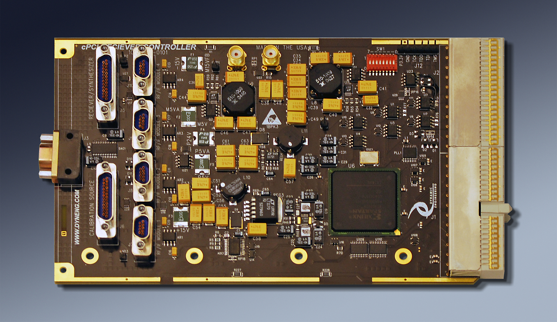
cPCI Receiver Controller
cPCI module with Digital Receiver Interface
Order This Item
Please contact sales@dyneng.com for this item.cPCI Receiver Controller Description
cPCI Receiver Controller
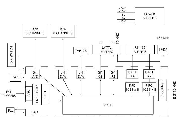
cPCI Receiver Controller Simplified Block Diagram
This design is from 2008. The design has been migrated to the VPX platform with the latest version called VPX-GLIB. The intermediate version was called VPX-RCB. If your project requires cPCI or some of the unique features of this version we can bring the design forward to be manufacturable with current devices etc.
The cPCI Receiver Controller is a 3U 4HP design that can be used for many purposes. The primary design implementation is to act as the controller slice within a digital receiver. The host computer can access the Receiver Controller over the PCI bus within the cPCI system. The Receiver Controller buffers commands from the host and converts them to the appropriate format to interface with the rest of the Digital Receiver. The initial design is controlled with several SPI [Serial Peripheral Interface] buses.
The Receiver Synthesizer and Calibration Source interfaces have unusual 2 bit parallel SPI buses with programmable length [1-32 bits] operating at 20 MHz. The on board A/D uses an SPI bus to task and return data. The DAC uses an SPI bus to program the channel and value to output. An on-board temperature sensor is provided and it is accessed with a 5th SPI bus. The hardware takes care of storing the command, conversion, and interaction with the device. Status is provided to indicate when additional commands can be sent or when data is available.
Each of the SPI buses is controlled within the FPGA and separately buffered with 24 mA LVTTL line drivers. The FPGA logic is programmable to allow new definitions for each of the SPI buses or new buses altogether.
The ADC is implemented with an 8 channel device. The ADC is tasked with the SPI bus. The host selects the channel it wants to convert. The bus tasks the ADC with the channel number, and options for single ended or differential measurement, unipolar or bipolar encoding, and power options. When the conversion is completed the hardware reads the data back from the ADC and stores it into the FPGA to be read by the host CPU. A valid bit is set when the new data is stored. The channel pairs are routed for differential operation and can be used as single ended. The lower channels have a divider implemented to allow measurements above the 4.096V reference [18V]. The upper channels have options for open detection.
The DAC is implemented with an 8 channel device. Each channel has an inverting buffer. The output swings from 0V to minus 3V to control the attenuators within the receiver. Two are provided per channel connector. The DAC is tasked with the SPI bus. The host selects the channel it wants to convert. The bus tasks the ADC with the channel number and value to output. A valid bit is set when the new data is stored. Individual channels and groups of channels can be set in parallel.
Texas Instruments TMP123 is used to measure the local temperature on the surface of the board near the FPGA. The sensor is read with an SPI bus. A write to the port causes a conversion to take place. A read from the port retrieves the data - already converted and stored. Conversion status is provided. The temperature range is -40 to +125C. The measurements are within 2C, and within 1.5C for a reduced range of -25C to +85C.
The Digital Receiver requires several voltages. The cPCI backplane supplies 5V to the cPCI Receiver Controller. The 5V is converted to the local voltages required [1.2, 2.5, 3.3] and to +/-15, +24, -5 to support the other receiver functions. The power provided to the rest of the receiver is fuse protected with self-healing fuses. The alternate voltages are converted using efficient switching power supplies. Filtering is provided to on each rail to provide clean power.
A UART with differential IO is provided for serial communications. The UART is supported with deep FIFOs on TX and RX sides. [1023 x 8]. The parity and stop bits are programmable. The frequency is programmable. The baud rate is based on an 18.432 MHz reference provided by the on-board PLL and divided locally under SW control. All of the standard rates can be selected, and by changing the PLL reference custom ones can be attained. The transceivers are rated to 40 MHz. The RX side uses a 16x clock and could be programmed to operate at baud rates near 12.5 MHz.
Two SMA connectors are supplied with a 10 MHz clock reference. The signal is LVTTL. A mini-DB9 connector is supplied with 125 MHz LVDS for an additional reference clock. The initial reference for the 10 MHz and 125 Mhz can be from an external reference or from the local oscillator. In the case of the oscillator a 50 MHz signal is upconverted to 100 MHz. The 100 Mhz is used as a reference within the design to generate 20 MHz, 10 MHz, 2 MHz for the SPI buses. The 10 Mhz is muxed to be the internally generated version or the external version. The 10 MHz is then upconverted to create the 125 MHz. A dual counter is provided with control from SW to capture a known count with the internally generated 10 MHz and the external 10 MHz for comparison purposes - signal present and accuracy.
There are 24 LVTTL buffers, 7 RS-485 transceivers and 1 LVDS transceiver used within the Receiver Controller. The transceivers are programmable for direction. The transceivers are set to the directions required for the initial design and can be modified for other requirements. For example and external 125 MHz clock could be received by the LVDS buffer and brought into the design. Some of the LVTTL buffers are used in parallel making a total of 18 unique signals. One signal is buffered to all 6 of the communications connectors.
The universal PCI interface is 32/33 and can support DMA. The base design is register accessed.
The FPGA is a Xilinx Spartan 3 2000 with plenty of uncommitted gates to expand capabilities, and add new features. For example it is planned to add the FPGA CPU capability in the future. Most of the block RAM is available for new functions. Cables, Breakouts, and custom cables available. Detailed Hardware manual [PDF] available for download at the bottom of this page.
cPCI Receiver Controller Features
Size
3U cPCI 4 HP basic profile. Effectively taller when inter-module cables connected.
Communications connectors
2 x 25 microD, 4x9 microD
Clock Reference Connectors
2 x SMA [10 MHz LVTTL], 1x9 pin microD [1 x 125 MHz LVDS]
Receiver Synthesizer IF
Micro 25 D, SPI bus, 24V, 15V, -15V, -5V, 5V, 3 TTL control signals, 1 differential ADC input.
Calibration Source IF
Micro 25 D, SPI bus, 24V, 15V, -15V, -5V, 5V, 3 TTL control signals, 1 differential ADC input.
RF/IF Module IF
4-9 pin micro D connectors each with 2 attenuation controls, master strobe, +5V, -5V
J2
Rear Panel IO with 2 differential ADC inputs, 3 LVTTL inputs with COS and time-tag, 10 MHz reference clock input, 4 bit differential bus for antenna band selection, UART RX/TX differential, 4 LVTTL buffered outputs.
Differential IO
7 - RS-485 differential transceivers. Each with programmable direction and data. 40 MHz max rate. 1 LVDS transceiver. Matched length impedance controlled routing.
Interrupts
INTA on PCI bus.
Power
5V on PCI connector. Internal voltages generated on board with switching power supplies. Fused Filtered power +24, +/-15V, +/-5V.
PCI VIO
Universal Voltage design
Specification
PCI specification compliant.
Specification
PLL plus FPGA DCMs can be programmed to provide accurate software controlled IO rates.
DIP Switch
8 position switch are provided to allow for configuration control.
JTAG
JTAG connections are tied to a labeled header. FPGA programming can be updated in the field.
cPCI Receiver Controller Benefits
Speed
The cPCI-Receiver Controller offers PCI speeds and direct register access to each control or status bit.
Price
The cPCI-Receiver Controller can save you time and money with easy-to-use hardware available at a reasonable cost. Custom and off-the-shelf cable systems will help with a low overall system cost. Quantity discounts are available.
Ease of Use
The cPCI-Receiver Controller is easy to use. Direct mapped hardware with minimized set-up requirements. Full size registers with read-back. Valid status for time delayed operations. The engineering kit provides a good starting point for a new user.
Availability
The cPCI-Receiver Controller is made to order in most cases. Usually, new customers will also have new requirements, which require changing the programming within the FPGA. If you need a custom version, Dynamic Engineering can send the base model now, update the VHDL, and send a new programming file that can be installed via the built-in JTAG FLASH programming capability. With the modular design approach and spare room within the FPGA, Dynamic Engineering can make changes rapidly and have a newly defined version ready for you in a short period of time.
Size
3U 4HP is the basic size. The 2 micro D 25, 4 micro D 9, and 2 SMA connectors are oriented [vertical] for cables to be used to interconnect with other modules within the receiver design. The effective height may be more than 4HP when the cables are connected
PCI Compatibility
cPCI-Receiver Controller is a PCI compliant device. The cPCI-Receiver Controller can be expected to work in any cPCI compliant backplane.
Part Number: cPCI-Receiver Controller
Ordering Options
- cPCI-Receiver Controller Standard board - with 3 IP positions, Industrial temperature components. Add any of the following build options after the PN as shown below:
- -ROHS Use ROHS processing. Standard processing is "leaded"
- -CC Option to add Conformal Coating
cPCI-ReceiverController Drivers
Software Support for cPCI-ReceiverController includes: Windows® compliant drivers
Please see the Driver manuals for the specifics of each type.
Integration support is available. Please contact Dynamic Engineering for this option or download the Technical Support Description from the Company button.
Please see the Driver manuals for the specifics of each type.
Integration support is available. Please contact Dynamic Engineering for this option or download the Technical Support Description from the Company button.
cPCI-ReceiverController Manuals
Click on the link to Download selected manuals in PDF format.
Download the cPCI Receiver Controller Model CSS1 manual revision B
Download the cPCI Receiver Controller Model CSS1 manual revision B