PCIe104Diff
PCIe104 Compatible Multi Function Interface
PCIe104Diff Description
- Standard PCIe-104 module
- PCIe single lane operation
- 18 Independent differential IO. Each with programmable termination and direction.
- RS-485, RS-422, LVDS, and mixed electrical standards
- LFE3-35EA Lattice FPGA with BRAM for FIFO or RAM implementation
- Programmable PLL clock references
- 1 year warranty standard. Extended warranty available.
- Extended [Industrial] Temperature standard.
- ROHS and Standard processing available
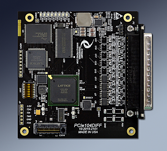
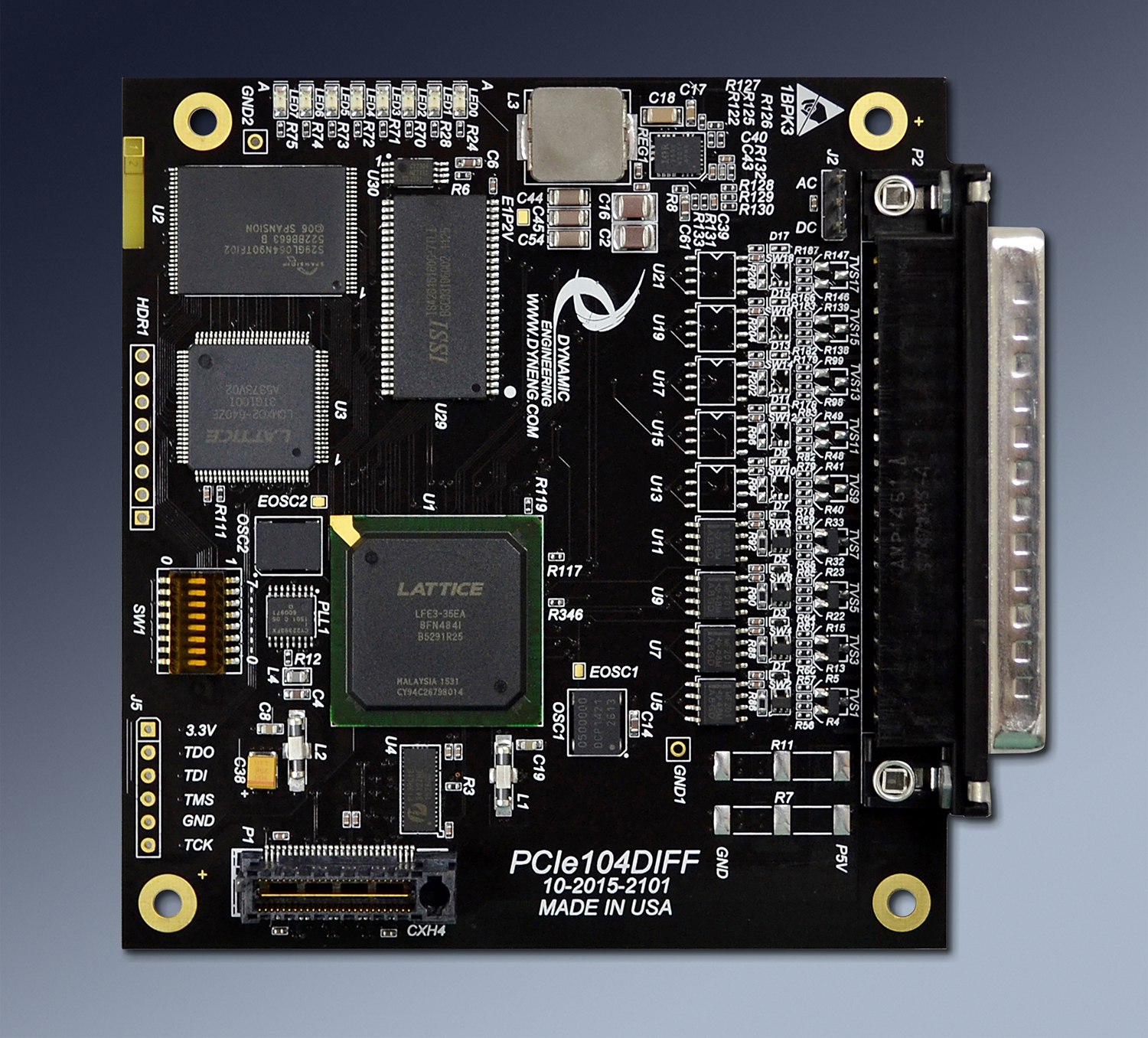
PCIe104Diff is a native PCIexpress based interface design based on the PC104 stacking concept. PCIe104 adds the PCIe interface and removes the legacy ISA interface. The stacking connectors can be seen on the lower left side of the title image. PCIe104Diff is a minimized "BiSerial" design intended for single or simple multi-channel designs. The IO connector is a DB37. 18 differential pairs are available in RS485, LVDS or combinations. Analog switches allow for programmable terminations. Half-Duplex, Full-Duplex, and uni-directional systems can be configured with software and VHDL.
The 18 IO can be configured to support one function, one function replicated several times, or multiple functions. For example the "RL1" has 8 UART channels, while the "ORB2" has 8 channels with 4 different functions. A real space saver when you need to have some Manchester to go with your UART and HDLC ports. A partial list of functions implemented in "Channels" includes: Manchester, Miller, SDLC, UART, Serial, Parallel, GPIO, COS, Custom, LADEE, NMS, Camera, Ternary, Low Speed, High Speed, Telemetry, Master & Target interactive IO, Adaptive. To support the functions, the designs include: memory elements instantiated with FIFO, Dual Port RAM, register files, as well as state-machines, counters, timers, dividers, registers, CRC and Parity generation/checking, software drivers and applications, DMA [Direct Memory Access] and the glue that goes with it. Our designs are all written in VHDL and done in a heirarchy allowing direct porting of different features to create new implementations. PCIe104Diff designs can use the extensive BiSerial VHDL library.
The hardware has been used to interface with a wide variety of equipment. What do you need to communicate with? Control? Capture data from? Please see the bottom of this page and other "Diff" implementations for descriptions and manuals for our customerized versions. We have been doing custom versions of the BiSerial since 1998 when the IP version first came out. We will be doing custom versions in the future with the next generation parts and features.
A new custom version can be implemented in a very reasonable time. Typically, a new design includes the new VHDL set, Windows® or Linux or VxWorks driver, reference software package, and documentation. Go to the 'Manuals' tab to see if the configuration you need already exists or if we need to work on a custom version for you.
Dynamic Engineering is quick to respond. Dynamic Engineering designs are structured to allow ports to be moved in and out facilitating rapid creation of new designs. Most of our implementations have a fairly large component of reused "known good" VHDL we can pull from allowing Dynamic Engineering to focus on the new functions required for your product specifications. You are getting the benefit of many man-years of design and test time with each new version created, which reduces risk and design time.
PCIe104Diff can be used along with a PCIe or other carrier/adapter to use with PCIe system or as a native PCIe104 card in a stack. Dynamic Engineering has a PCIe104 carrier for PCIexpress, and can do custom design´s specific to client requirements as well. Please use the handy JAVA pull-down menu at the top left of any page to navigate to other Dynamic Engineering products including carriers.
It all starts with the PCB [Printed Circuit Board]. Quality design and quality materials are required to meet the strenuous requirements of all of our implementations. The quality goes in before the parts go on. In addition to routing strategy and layer counts, via size, plating requirements, break-out trace widths, and materials are areas where quality comes into play. The via size and method of trace attachment to the via affect the signal shape and reliability. Using tear-drop trace connections to pads, vias and through hole components enhance the reliability and minimize the impedance discontinuity resulting in a cleaner signal. The design has several power planes with sufficient copper weight and coverage to provide the references required for the routing plus the current and voltages needed by the various devices on the board. The larger features make the design work more difficult since there is less room to "play with" and the end result is worth it. Since 1998 when the IP BiSerial was introduced, the BiSerial family has enjoyed an excellent track record for reliability.
The PCIe interface has a published set of requirements for compliance which restrict length, impedance, loading, and other factors. PCIe104Diff is compliant with the PCIe Specification adapted for PCIe104 stacks. The IO section has requirements based on the IO type and the purpose for the IO. A very conservative approach has been taken to allow operation with any client requirement. The IO can be LVDS or RS-485. The IO on the connector side is differential with a 100 ohm impedance requirement. Between the FPGA and the tranceivers the IO is single ended. Each IO has separate direction, termination, and data lines to allow complete flexibilty. The design has matched length connections from the FPGA ball to the seating plane of the connector. The lengths are matched to the "mil". The Impedance is controlled and the signals routed with proper spacing to avoid cross talk etc. The other features including memory, PLL, oscillator, and power supplies are implemented within the PCB to exceed the operational requirements for those devices.
The Lattice FPGA has internal block RAM which can be configured in a variety of ways including FIFO and Dual Port RAM. Dual Port RAM can be utilized to allow direct addressing and retransmission of repeated patterns.
Sometimes you just need more memory. 16Mx16 of SDRAM is provided. With VHDL the SDRAM interface can be modified for specific requirements. The base implementation is as a large programmable FIFO. The amount of memory allocated to Tx and Rx functions is programmable. The Memory is designed to be 4 ported with DMA in, DMA out, Transmit and Receive ports. Each of the ports has a built in block RAM FIFO to support refresh, other ports using the memory, and rate matching. Internal loop-back is supported. The loop-back test can be used for BIT and for software development. Programmable FIFO flags are supported on both sets of FIFOs. Programmable Almost Full, Programmable Almost Empty, plus Full, Half Full, and Empty. The programmable flags can be set to any depth to allow the software a programmable delay from event to empty or full. The interrupts can be very useful when sending or receiving messages larger than the FIFO size. The interrupts are programmable and provisions are made to allow polling. In addition DMA can be programmed to fill or empty the FIFO with sizes larger than the FIFO size. The DMA is hardware controlled to be held off when no data is available or no room is available. With the "Channelized DMA"™ capability and large FIFOs the software application can have reduced interrupt counts to deal with while supporting larger and faster IO transfer rates.
PCIe104Diff has 18 transceivers which can be used for any combination of input and output functions. Parallel and serial data, multiple channels, and different hand-shaking schemes can be implemented with the quantity of IO on the PMC-BiSerial. RS-485 transceivers support up to 50 MHz rates. The LVDS transceivers are rated at better than 200 MHz.
The IO is available through the DB37 connector. Each transceiver pair is isolated from the connector with zero ohm resistors. The resistors can be changed out to support your particular interface requirements. In addition, the IO have resistors tied between the IO and a power plane. The plane is strappable to allow 5V or GND on either rail. The IO can be set to provide a high or a low condition when not driven to support half duplex operation without adding resistors to your cables.
Clock options are frequently a major factor in embedded designs. Getting the right reference to the right part of the design and allowing for local control of exact frequencies. PCIe104Diff has a PLL with 2 programmable outputs, reference oscillator, internal DCMs and buffering plus programable dividers instantiated within the VHDL. The PLL can be programmed to any fixed frequency, the DCM used to create phase variations, and local dividers to allow on-the-fly channel based frequency changes.
"Channelized DMA"™ is an important feature of the PCIe104Diff design.With "Channelized DMA"™ you have a separate DMA engine for each transmitter and each receiver within each channel. Each state-machine can be serviced independently with DMA without requiring intervention from the host. Large data transfers can happen between multiple connections while the CPU is off doing something else. In non-channelized designs the CPU will have to intervene each time a different port needs to be serviced. With a channelized approach the hardware takes care of the local arbitration, and eliminates the intervention for better system performance and less latency.
If your situation demands a custom application, we will update the Lattice FPGA and IO components. Send us your timing and we will send you the interface. Please refer to the 'Manuals' tab for completed PCIe104Diff implementations.
Email us your wish list or call today.
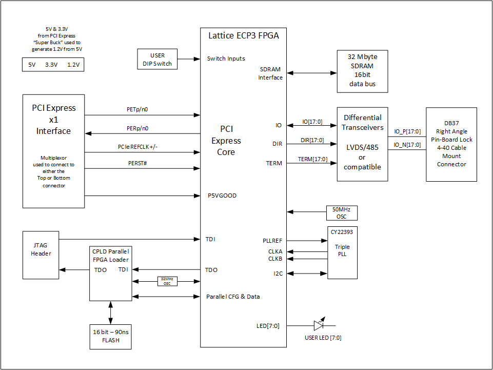
PCIe104Diff Block Diagram

The 18 IO can be configured to support one function, one function replicated several times, or multiple functions. For example the "RL1" has 8 UART channels, while the "ORB2" has 8 channels with 4 different functions. A real space saver when you need to have some Manchester to go with your UART and HDLC ports. A partial list of functions implemented in "Channels" includes: Manchester, Miller, SDLC, UART, Serial, Parallel, GPIO, COS, Custom, LADEE, NMS, Camera, Ternary, Low Speed, High Speed, Telemetry, Master & Target interactive IO, Adaptive. To support the functions, the designs include: memory elements instantiated with FIFO, Dual Port RAM, register files, as well as state-machines, counters, timers, dividers, registers, CRC and Parity generation/checking, software drivers and applications, DMA [Direct Memory Access] and the glue that goes with it. Our designs are all written in VHDL and done in a heirarchy allowing direct porting of different features to create new implementations. PCIe104Diff designs can use the extensive BiSerial VHDL library.
The hardware has been used to interface with a wide variety of equipment. What do you need to communicate with? Control? Capture data from? Please see the bottom of this page and other "Diff" implementations for descriptions and manuals for our customerized versions. We have been doing custom versions of the BiSerial since 1998 when the IP version first came out. We will be doing custom versions in the future with the next generation parts and features.
A new custom version can be implemented in a very reasonable time. Typically, a new design includes the new VHDL set, Windows® or Linux or VxWorks driver, reference software package, and documentation. Go to the 'Manuals' tab to see if the configuration you need already exists or if we need to work on a custom version for you.
Dynamic Engineering is quick to respond. Dynamic Engineering designs are structured to allow ports to be moved in and out facilitating rapid creation of new designs. Most of our implementations have a fairly large component of reused "known good" VHDL we can pull from allowing Dynamic Engineering to focus on the new functions required for your product specifications. You are getting the benefit of many man-years of design and test time with each new version created, which reduces risk and design time.
PCIe104Diff can be used along with a PCIe or other carrier/adapter to use with PCIe system or as a native PCIe104 card in a stack. Dynamic Engineering has a PCIe104 carrier for PCIexpress, and can do custom design´s specific to client requirements as well. Please use the handy JAVA pull-down menu at the top left of any page to navigate to other Dynamic Engineering products including carriers.
It all starts with the PCB [Printed Circuit Board]. Quality design and quality materials are required to meet the strenuous requirements of all of our implementations. The quality goes in before the parts go on. In addition to routing strategy and layer counts, via size, plating requirements, break-out trace widths, and materials are areas where quality comes into play. The via size and method of trace attachment to the via affect the signal shape and reliability. Using tear-drop trace connections to pads, vias and through hole components enhance the reliability and minimize the impedance discontinuity resulting in a cleaner signal. The design has several power planes with sufficient copper weight and coverage to provide the references required for the routing plus the current and voltages needed by the various devices on the board. The larger features make the design work more difficult since there is less room to "play with" and the end result is worth it. Since 1998 when the IP BiSerial was introduced, the BiSerial family has enjoyed an excellent track record for reliability.
The PCIe interface has a published set of requirements for compliance which restrict length, impedance, loading, and other factors. PCIe104Diff is compliant with the PCIe Specification adapted for PCIe104 stacks. The IO section has requirements based on the IO type and the purpose for the IO. A very conservative approach has been taken to allow operation with any client requirement. The IO can be LVDS or RS-485. The IO on the connector side is differential with a 100 ohm impedance requirement. Between the FPGA and the tranceivers the IO is single ended. Each IO has separate direction, termination, and data lines to allow complete flexibilty. The design has matched length connections from the FPGA ball to the seating plane of the connector. The lengths are matched to the "mil". The Impedance is controlled and the signals routed with proper spacing to avoid cross talk etc. The other features including memory, PLL, oscillator, and power supplies are implemented within the PCB to exceed the operational requirements for those devices.
The Lattice FPGA has internal block RAM which can be configured in a variety of ways including FIFO and Dual Port RAM. Dual Port RAM can be utilized to allow direct addressing and retransmission of repeated patterns.
Sometimes you just need more memory. 16Mx16 of SDRAM is provided. With VHDL the SDRAM interface can be modified for specific requirements. The base implementation is as a large programmable FIFO. The amount of memory allocated to Tx and Rx functions is programmable. The Memory is designed to be 4 ported with DMA in, DMA out, Transmit and Receive ports. Each of the ports has a built in block RAM FIFO to support refresh, other ports using the memory, and rate matching. Internal loop-back is supported. The loop-back test can be used for BIT and for software development. Programmable FIFO flags are supported on both sets of FIFOs. Programmable Almost Full, Programmable Almost Empty, plus Full, Half Full, and Empty. The programmable flags can be set to any depth to allow the software a programmable delay from event to empty or full. The interrupts can be very useful when sending or receiving messages larger than the FIFO size. The interrupts are programmable and provisions are made to allow polling. In addition DMA can be programmed to fill or empty the FIFO with sizes larger than the FIFO size. The DMA is hardware controlled to be held off when no data is available or no room is available. With the "Channelized DMA"™ capability and large FIFOs the software application can have reduced interrupt counts to deal with while supporting larger and faster IO transfer rates.
PCIe104Diff has 18 transceivers which can be used for any combination of input and output functions. Parallel and serial data, multiple channels, and different hand-shaking schemes can be implemented with the quantity of IO on the PMC-BiSerial. RS-485 transceivers support up to 50 MHz rates. The LVDS transceivers are rated at better than 200 MHz.
The IO is available through the DB37 connector. Each transceiver pair is isolated from the connector with zero ohm resistors. The resistors can be changed out to support your particular interface requirements. In addition, the IO have resistors tied between the IO and a power plane. The plane is strappable to allow 5V or GND on either rail. The IO can be set to provide a high or a low condition when not driven to support half duplex operation without adding resistors to your cables.
Clock options are frequently a major factor in embedded designs. Getting the right reference to the right part of the design and allowing for local control of exact frequencies. PCIe104Diff has a PLL with 2 programmable outputs, reference oscillator, internal DCMs and buffering plus programable dividers instantiated within the VHDL. The PLL can be programmed to any fixed frequency, the DCM used to create phase variations, and local dividers to allow on-the-fly channel based frequency changes.
"Channelized DMA"™ is an important feature of the PCIe104Diff design.With "Channelized DMA"™ you have a separate DMA engine for each transmitter and each receiver within each channel. Each state-machine can be serviced independently with DMA without requiring intervention from the host. Large data transfers can happen between multiple connections while the CPU is off doing something else. In non-channelized designs the CPU will have to intervene each time a different port needs to be serviced. With a channelized approach the hardware takes care of the local arbitration, and eliminates the intervention for better system performance and less latency.
If your situation demands a custom application, we will update the Lattice FPGA and IO components. Send us your timing and we will send you the interface. Please refer to the 'Manuals' tab for completed PCIe104Diff implementations.
Email us your wish list or call today.

PCIe104Diff Features
Interface Types
Custom programmed interfaces are available. Please send us a timing diagram, and we can program one for you. Most interfaces can be adapted from our large library of designs including the updated VHDL, Windows or Linux or VxWorks Driver, reference manuals etc. We can support on-site [ours] integration to help you get your application level software working.
Signaling
18 RS-485 / RS-422 / LVDS compatible IO are provided. Any combination of transmit or receive channels can be created. LVDS and RS-485 can be mixed. Programmable termination. Pull-up and Pull-down option on IO to allow controlled level when tri-stated. Option for marking or low state.
IO
The IO is available via the DB37 connector. The differential IO is properly routed with impedance control, pitch, and space plus matched lengths across all of the pairs.
Transmit Speeds and Clocking
Up to 50 MHz RS485, and up to 200 MHz LVDS signaling supported. 2 programmable PLL inputs. Reference oscillator. Counters/Dividers/DCM for local clock control.
PCIe Speed
Single lane PCIe 1 operation Standard Target accesses, and "Channelized DMA"™ supported. "Channelized DMA"™ is a full DMA capability on each function in a multi-function implementation.
Software Interface
Registers are read-writeable. VxWorks, Linux and Windows® drivers available. Design help for alternate OS implementations.
DIP Switch
An 8 bit DIP Switch is provided for user purposes. The DIP switch can be used to allow the application software to positively identify a PCIe104Diff in a multi-board implementation.
Interrupts
Software programmable interrupts on status, errors, completion of transfer, DMA, FIFO levels, custom events. Status can be polled for non-interrupt driven operation as well.
Memory
Separate FIFOs/Dual Port RAM are provided for all channels. Internal FPGA Block RAM memory modules for fast access. SDRAM 16Mx16 included.
FPGA
Lattice LFE3 series. FLASH is used to program the FPGA. In many cases any feature updates can be sent to your facility to reprogram without down time.
Power
5V and 3.3V used from PCIe104 connector.
Temperature
Industrial Temperature is standard. [-40 to +85].
Assembly
Standard [leaded] processing or ROHS compliant processing are available. See ordering options.
Conformal Coating
Conformal Coating is available to support operation in condensing environments.
Size
Standard PCIe104
STEP
STEP files are available to support your system integration. Please contact sales@dyneng.com for this option.
PCIe104Diff Benefits
Speed
PCIe104Diff is optimized for differential interfacing requirements. The FIFO memories and programmable interrupts off-load the CPU from most of the management other implementations require. FIFO access is optimized for the PCIe bus further reducing overhead by speeding up the data transfer. On the IO side, PCIe104Diff has independent channel functions. Channels can operate at maximum rate in parallel.
Price
PCIe104Diff is easily programmed to implement new functions. Many previously implemented "custom designs" are available too. Without the costs of schematic level design, layout, debugging etc., a modified PCIe104Diff will represent a large cost savings.
Ease of Use
PCIe104Diff is easy to use. The registers are designed to be R/W without layering or other indirect control methods. Use the Dynamic Engineering Driver with Windows® VxWorks, or Linux or create your own. In most cases the interfaces are "Point and shoot" - just fill the memory and set the start bit to get your custom protocol transmitting. The driver and user application reference software have built-in utilities for parsing new PLL frequency files, loading the PLL, reading the switch, doing loop-back using DMA via the IO.
Availability
We work to keep PCIe104Diff in stock. Dynamic Engineering can build and deliver products fast through in-house manufacturing capabilities.
Size
PCIe104Diff is a standard PCIe104 card and meets the PCIe104 mechanical specifications.
PCIe104 Compatibility
PCIe104Diff is a PCIe104 Compliant per the PCIe104 specification.
PCIe Compatibility
PCIe104Diff is PCIe compliant. You can develop with PCIe1LPCIe104.
Part Number: PCIe104Diff
Ordering Options
- Due to the number of options for building and configuring PCIe104Diff is a quoted item. Please contact Dynamic Engineering with your requirements or the name of the model if one already exists that meets your needs.
PCIe104Diff Drivers
Software Support for PCIe104Diff includes: Windows®, VxWorks, and Linux compliant drivers
Please see the Driver manuals for the specifics of each type.
Drivers and Reference SW are developed for each type/version of PCIe104Diff implemented. When custom versions are ordered the NRE will include providing Windows, Linux, and or VxWorks packages. For off-the-shelf models, select on the manuals tab, the Windows® and Linux SW shown is included with your purchase of the HW. A small one-time charge is required for the VxWorks versions. Unsupported SW versions may have an NRE requirement.
Integration support is available. Please contact Dynamic Engineering for this option or download the Technical Support Description from the Company button.
PCIe104Diff Manuals
Click on the link to Download selected manuals in PDF format.
Download the PCIe104Diff OS1 Hardware Manual
Download the IP Carrier Windows®10 manual. PCIe104Diff OS1 Linux manual.
Download the PCIe104Diff Statement of Volatility
Download the PCIe104Diff OS1 Hardware Manual
Download the IP Carrier Windows®10 manual. PCIe104Diff OS1 Linux manual.
Download the PCIe104Diff Statement of Volatility


