VPX Receiver Controller
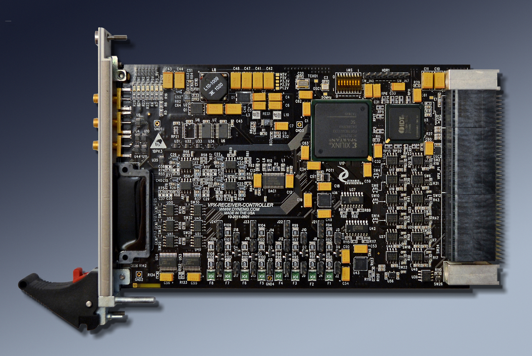
VPX Module with Receiver Controller Interface
Order This Item
Please contact sales@dyneng.com for this item.VPX Receiver Controller Description
VPX Receiver Controller

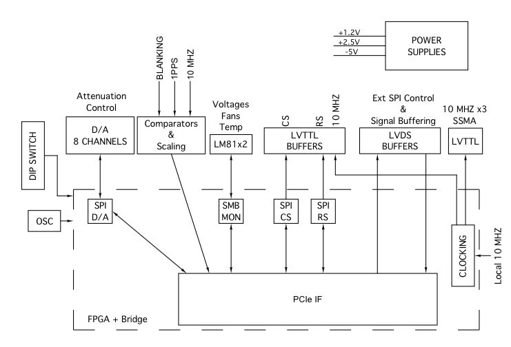
VPX Receiver Controller Simplified Block Diagram
VPX Receiver Controller is a 3U 4HP design that can be used for many purposes. The primary design implementation is to act as the controller slice within a digital receiver. The host computer can access the Receiver Controller over the PCIe bus within the VPX system or using the SPI bus available from P2. The Receiver Controller buffers commands from the host and converts them to the appropriate format to interface with the rest of the Digital Receiver. The initial design is controlled with several SPI [Serial Peripheral Interface] and SMB buses.
The host SPI connection to VPX-RCB is augmented with a 3 bit parallel address and master enable signal. The address bits allow VPX-RCB to determine the destination to be driven or read. Data is automatically redirected to the end point and enables asserted to support the transfer. In the case of the SMB connections VPX-RCB automatically converts the full duplex SPI bus into the half duplex SMB protocol. Addressing embedded within the SPI traffic allows direct control of the local devices. The internal [FPGA] registers are dual accessible to allow the PCIe bus to interact with these as well. Each of the SPI buses is controlled within the FPGA and separately buffered with 24 mA LVTTL line drivers. The FPGA logic is programmable to allow new definitions for each of the SPI buses or new buses altogether.
The Receiver Synthesizer and Calibration Source interfaces are supported with a total of 4 SPI buses controlled by the host and buffered by the VPX-RCB. The DAC uses an SPI bus to program the channel and value to output. The monitor circuits are on the SMB and provide temperature, voltage, and Fan speed information. The internal and several external voltages are measured.
The DAC is implemented with an 8 channel device. Each channel has an inverting buffer. The output swings from 0V to minus 3V to control the attenuators within the receiver. The 8 attenuators are available on the 69 pin high density connector at the front panel. The DAC is tasked with the SPI bus. The host selects the channel it wants to convert. Individual channels and groups of channels can be set in parallel. The DAC is centered in the photo with the opamps to the left. The pin definitions on the communication connector are designed to allow the analog ground reference to cover the attenuation signals from the DAC through the opamps and to the connector. Please refer to the HW manual for the pinout.
Two Texas Instruments LM81s are used to measure the local temperature on the surface of the board as well as provide the voltage monitoring and fan measurement functions. Please see the HW manual for details of the voltages measured and the scaling used.
Three SSMA connectors are supplied with a 10 MHz clock reference. The signal is LVTTL. The reference for the 10 MHz can be from an external reference or from the local TCXO. A dual counter is provided with control from SW to capture a known count with the internally generated 10 MHz and the external 10 MHz for comparison purposes - signal present and accuracy. The limits of the acceptable counts for the time programmed can be set. The time is based on the local 100 MHz clock. Status is provided where "good" means above the lower limit and below the upper limit. The tests run automatically. An interrupt is available if the status changes.
LED´s are provided to indicate the PCIe lanes acquired plus basic voltage status. EPADs are also provided to measure voltages and reference frequencies.
Four special purpose inputs are available. The initial use is for Blanking signals which can be single ended or differential, low voltage or high voltage. The four channels have differential signal routing with 1/2 W shunt selectable resistive elements to allow operation from high voltages or low. You can see the circuits basically centered along the lower edge of the board in the photo.The four channels have shunt selectable 100 ohm parallel terminations [can be populated with a different value...] or a digitial pot programmed reference voltage or open. The signal is passed to a high speed comparator [4 channel] with 700 pS delay. The comparator can handle +/-5V signals. The received signals are diode coupled to the power rails to prevent over and under voltage issues. The signals are currently routed through the FPGA and converted to LVDS to be redriven to the P2 connector for the local host CPU. The FPGA can have added signal processing etc. added for these and other signals.
There are multiple LVTTL buffers, LVDS transceivers, and RS-485 transceivers used within the Receiver Controller. The transceivers are programmable for direction and termination. The transceivers are set to the directions required for the initial design and can be modified for other requirements.
The universal PCI interface on the FPGA is 32/33 and can support DMA. The base design is register accessed. The bridge supports both DMA and target access types. SPI control from the host is the expected initial control path
The FPGA is a Xilinx Spartan 3 2000 with plenty of uncommitted gates to expand capabilities, and add new features. The FLASH is set-up to handle a 4000 level device if needed. For example it is planned to add the FPGA CPU capability in the future. Most of the block RAM is available for new functions. Cables, Breakouts, and custom cables available. Detailed Hardware manual [PDF] available for download at the bottom of this page.
VPX Receiver Controller Features
Size
VPX 3U 4 HP basic profile.
Communications connectors
P2 on rear panel, plus 69 pin high density avionics connector on front bezel
Clock Reference Connectors
3 x SSMA [10 MHz LVTTL]
Receiver Synthesizer IF
SPI x 2 plus voltage monitoring and 8 attenuation signals
Calibration Source IF
SPI x 2 plus voltage monitoring
RF/IF Module IF
Antenna control IO - RS485
J2
Rear Panel IO with 2 differential ADC inputs, 3 LVTTL inputs with COS and time-tag, 10 MHz reference clock input, 4 bit differential bus for antenna band selection, UART RX/TX differential, 4 LVTTL buffered outputs.
Differential IO
7 - RS-485 differential transceivers. 40 MHz max rate. LVDS transceivers - 200 mhz. Matched length impedance controlled routing. Each with programmable Direction and Termination
Interrupts
INTA on PCI bus encoded via PCIe bus, and Attention via P2 to host CPU
Power
12, 5V, 3.3 on P0 connector. Internal voltages generated on board with switching power supplies. [-5V, 1.2V, 2.5V]
Specification
VPX, PCIe & PCI specification compliant
PCIe Clock
Since the VPX standard does not distribute the PCIe clock as a standard PC does, VPX-RCB has a local 100 MHz reference oscillator for synchronization purposes. Non-Spread Spectrum clocking can be used with this board. Next revision to include REF CLK option.
DIP Switch
8 position switch are provided to allow for configuration control.
JTAG
JTAG connections are tied to a labeled header. FPGA programming can be updated in the field.
VPX Receiver Controller Benefits
Speed
VPX-RCB offers PCIe speeds and direct register access to each control or status bit
Price
VPX-RCB can save you time and money with easy to use hardware available at a reasonable cost. Custom and off-the-shelf cable systems will help with a low overal system cost.
Ease of Use
VPX-RCB is easy to use. Direct mapped hardware with minimized set-up requirements. Full size registers with read-back. Alternate SPI controlled operation via P2 to allow a local CPU high speed direct access without PCIe encoding delays.
Availability
VPX-RCB is made to order in most cases. Usually new customers will also have new requirements which require changing the programming within the FPGA. If you need a custom version we can send the base model now, update the VHDL and send a new programming file that can be installed via the built in JTAG FLASH programming capability. With our modular design approach and spare room within the FPGA we can make changes rapidly and have a newly defined version ready for you.
Size
3U 4HP is the basic size.
PCI/PCIe Compatibility
PCI /PCIe compliant. VPX-RCB can be expected to work in any VPX compliant backplane (see note above for spread spectrum clocking)
Part Number: VPX-RCB
Ordering Options
- VPX-Receiver Controller Standard board Add any of the following build options after the PN as shown below:
- -ROHS Use ROHS processing. Standard processing is "leaded"
- -CC Option to add Conformal Coating
VPX-RCB Drivers
Software Support for VPX-ReceiverController includes: Windows® compliant drivers Linux and VxWorks options.
Please see the Driver manuals for the specifics of each type.
Integration support is available. Please contact Dynamic Engineering for this option or download the Technical Support Description from the Company button.
Please see the Driver manuals for the specifics of each type.
Integration support is available. Please contact Dynamic Engineering for this option or download the Technical Support Description from the Company button.
VPX-RCB Manuals
Click on the link to Download selected manuals in PDF format.
Download the VPX Receiver Controller Hardware manual with memory and bit maps, IO definitions, theory of operation etc.
Download the VPX Receiver Controller Hardware manual with memory and bit maps, IO definitions, theory of operation etc.

